基于FPGA的微伏级直流电压测量系统的设计(附电路原理图)
来源:wenku7.com 资料编号:WK716606 资料等级:★★★★★ %E8%B5%84%E6%96%99%E7%BC%96%E5%8F%B7%EF%BC%9AWK716606
以下是资料介绍,如需要完整的请充值下载。
1.无需注册登录,支付后按照提示操作即可获取该资料.
2.资料以网页介绍的为准,下载后不会有水印.资料仅供学习参考之用. 密 保 惠 帮助
资料介绍
基于FPGA的微伏级直流电压测量系统的设计(附电路原理图)(论文10000字)
摘要:本文在分析研究传统微伏级直流电压信号测量的基础上,利用FPGA设计了微伏级直流电压信号测量系统。系统由信号放大,16位模数转换,LCD实时显示等模块构成。将采集的微伏级信号进行放大,通过AD转化成数字量,经I2C总线传输,在Quartus II平台上运用SOPC技术内嵌的处理器和IP核处理,最后经控制总线把数据展示在LCD液晶屏上。与传统直流电压信号测量系统相比,设计的测量系统体积小,可靠性较高,抗干扰强。实验结果证实了系统测量精度高,符合设计要求。
关键词:微伏级;测量;直流电压信号;FPGA
Design of microvolt DC voltage measurement system based on FPGA
Abstract:Based on the analysis of the traditional microvolt DC voltage signal measurement , the paper uses FPGA to design a microvolt DC voltage signal measurement system. The system is composed of a signal amplification module, a 16 bit analog to digital conversion module, a LCD real-time display module and so on. The collected microvolt signal is enlarged.Then it will be converted to digital by the AD module. And then we send the signal to FPGA core via the I2C bus.We use SOPC technology to embed processors and IP core in the Quartus II platform. Finally, the collected data are displayed on the LCD screen via control bus. Compared with the traditional DC voltage signal measurement system, the design of the measurement system is small in size, high in reliability and strong in anti-interference ability. The theoretical analysis and experimental results show that the measuring system has advantages with high accuracy, the rational design and so on.
Keywords:Microvolt; measure; dc voltage signal;FPGA
目 录
1 前言 3
1.1课题研究的背景和意义 3
1.2 直流电压信号测量的研究现状 4
1.3 设计要求 4
2 系统设计 4
2.1 系统主控芯片的选择与论证 4
2.2 信号放大模块的选择与论证 5
2.3 模拟-数字模块的选择与论证 5
2.4 显示模块的选择与论证 6
2.5 整体结构设计 6
3 硬件设计 6
3.1 信号放大模块 7
3.1.1 INA333仪表放大器 7
3.2 模拟-数字信号转化模块 8
3.2.1 Σ-Δ调制型 8
3.2.2 ADS1113 9
3.3 控制核心模块 10
3.4 显示模块 11
3.5 电源转换电路 12
3.5.1 FPGA部分供电 12
3.5.2 模拟电路部分供电 13
3.6 硬件电路参数设计 13
4 软件设计 14
4.3 Verilog与C相结合 14
4.4 软件整体结构框架 15
4.4.1 主体程序 15
5 实验测试 15
6 总结 16
参考文献 18
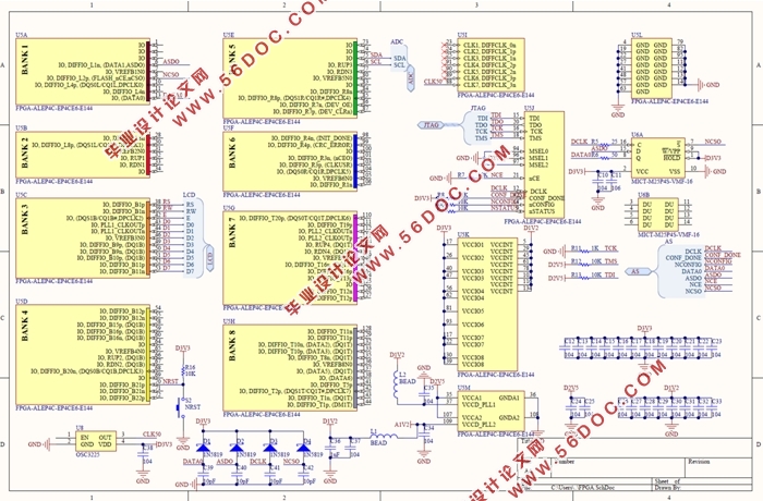
附录1 总电路原理图 19
附录2 硬件实物图 20
附录3 主要源程序 21
致谢 22
|