基于FPGA的多波形信号发生器设计(附电路图)
来源:wenku7.com 资料编号:WK716594 资料等级:★★★★★ %E8%B5%84%E6%96%99%E7%BC%96%E5%8F%B7%EF%BC%9AWK716594
以下是资料介绍,如需要完整的请充值下载。
1.无需注册登录,支付后按照提示操作即可获取该资料.
2.资料以网页介绍的为准,下载后不会有水印.资料仅供学习参考之用. 密 保 惠 帮助
资料介绍
基于FPGA的多波形信号发生器设计(附电路图)(论文12000字)
摘要:本文主要给出了基于FPGA的信号发生器的设计与实现过程。首先,以FPGA为核心设计了硬件系统,主要由FPGA模块、D/A模块、低通滤波器构成,其中,FPGA完成相位累加器的功能。其次,使用Quartus II软件进行Verilog程序编写,对时钟信号进行分频以及相位的累加,随后从LPM-ROM存储调用输出波形,再经过DA转换以及低通滤波器后输出波形。最后,将程序烧写进该硬件系统并调试。为提高实用性,本设计还添加了按键来选择输出波形种类,实现输出电压可调节、幅度可调节、频率可调节的功能。
关键词:信号发生器,现场可编程门阵列,DDS,Verilog语言
Multi waveform signal generator based on FPGA
Abstract:This paper mainly describes the design and implementation of signal generator based on FPGA.Firstly, the hardware system based on FPGA is designed, which is composed of FPGA module D/A module and low pass filter,and the function of phase accumulator completed by FPGA.Secondly, the Quartus II software is used to write the Verilog program, the clock signal is divided and the phase is accumulated, then the output waveform is called from the LPM-ROM storage, and then the waveform is output after the DA conversion and the low-pass filter.Finally, the program is written into the hardware system and debugged.In order to improve the practicability, the design also adds the key to select the type of output waveform to realize the output. The function of adjustable output voltage, adjustable amplitude and adjustable frequency.
Key words: signal Generator, Field Programmable Gate Array, DDS,Verilog language
目 录
第1章、绪论 1
1.1 背景与意义 1
1.2 国内外发展情况 1
1.3 任务及内容安排 2
第2章、系统的基本原理 3
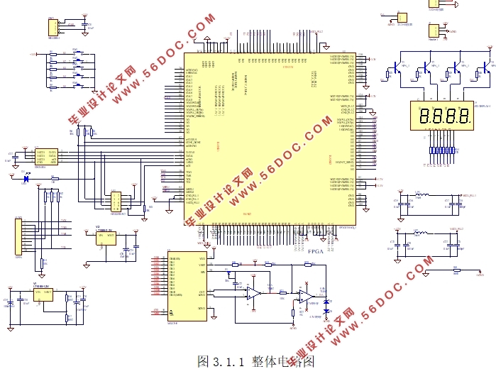
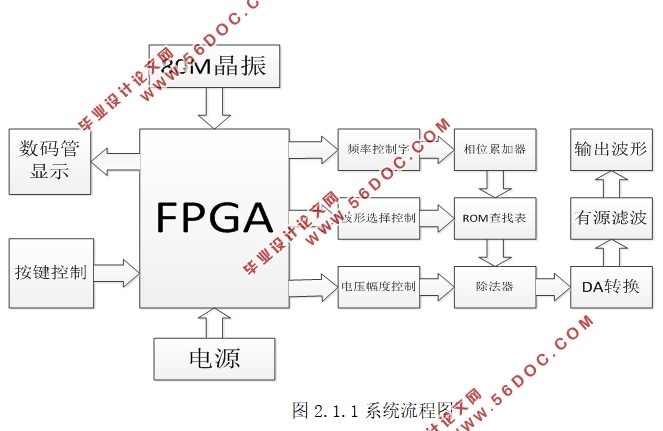
2.1 系统流程 3
2.2 频率合成技术 3
2.3 DDS基本原理 4
2.3.1DDS的优点 5
2.3.2DDS的缺点 6
2.4 FPGA基本原理 6
2.5 编程环境 6
2.6 Verilog语言 7
2.7仿真环境 7
第3章、硬件电路设计 8
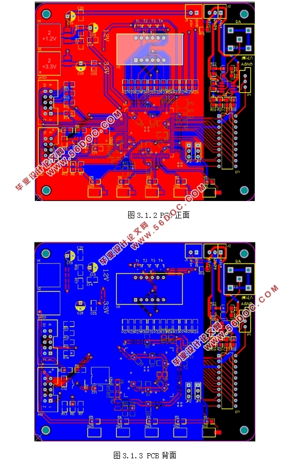
3.1 整体电路设计 8
3.2 FPGA外部电路设计 10
3.2.1 电源电路设计 10
3.2.2D/A转换电路设计 12
3.2.3 键盘控制电路设计 14
3.2.4 数码管显示电路设计 14
3.3.5 ROM存储电路设计 15
第4章、系统方案设计 16
4.1 整体方案的设计 16
4.2 DDS模块的方案 17
4.2.1 相位累加方案 17
4.2.2ROM存储方案 20
4.2.3 数模转换方案 21
4.2.4 低通滤波方案 23
第5章、 系统测试 23
5.1波形仿真 23
5.2实物演示 24
第6章、 总结与展望 27
参考文献: 27
致谢 29
|